Introdução
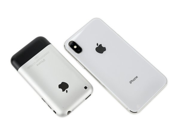
Ten years ago, Apple introduced the very first iPhone, and changed the world. Today, we're taking apart Apple's 18th iteration—the iPhone X. With its rounded edges and edge-to-edge display, we're sure this is the iPhone Steve imagined all of those years ago—but now that his dream is realized, will it be as influential as the first? Time will tell, but for now we'll be doing our part to help you decide. Join us as we open Apple's crown jewel to see what makes it shine.
A big thanks to Circuitwise for hosting our teardown down under, Creative Electron for X-ray imagery, and TechInsights for IC ID.
It's serendipitous that we're in Sydney, because we've got an Australia store now. As we learn more, we'll be posting on Facebook, Instagram and Twitter. We've got a newsletter too if you're the email type.
O que você precisa
Vídeo de Apresentação
-
-
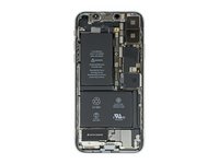
The iPhone X is here! Here's the fillin' inside that glass sandwich:
-
A11 "Bionic" chip with neural engine and embedded M11 motion coprocessor
-
5.8 inch "all-screen" OLED multitouch Super Retina HD display with 2436 × 1125-pixel resolution (458 ppi)
-
Dual 12 MP cameras (wide-angle and telephoto) with ƒ/1.8 and ƒ/2.4 apertures and OIS
-
7 MP TrueDepth camera with ƒ/2.2 aperture, 1080p HD video recording, and Face ID
-
Support for fast-charge and Qi wireless charging
-
Our A1865 global unit has broad cellular band support as well as 802.11a/b/g/n/ac Wi‑Fi w/MIMO + Bluetooth 5.0 + NFC.
-
-
-
The iPhone has come a long way in ten years—so long, in fact, that the design has cycled back a bit, and this iPhone looks more like the original than we've seen in a long time.
-
As was the case with the iPhone 8 earlier this year, Apple has banished the unsightly (and environmentally responsible) regulatory markings from the back of the iPhone X.
-
Jony finally has the featureless smooth backplane you know he's always wanted. Hopefully these phones still make it to recyclers without the hint and don't get dumped in the trash.
-
-
-
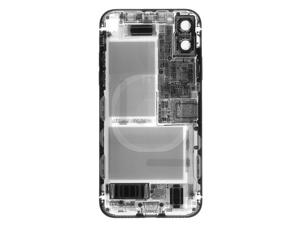
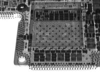
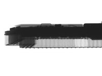
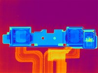
Before we dive in blindly, let's get some
10-rayX-ray recon from our friends at Creative Electron. -
Here's what we found:
-
Not one, but two battery cells. That's a first in an iPhone!
-
A super-tiny logic board footprint. Based on the overlaid solder points, it looks like there are two stacked layers.
-
To make room for the extra front-facing sensors, the earpiece speaker has been shifted down quite a bit.
-
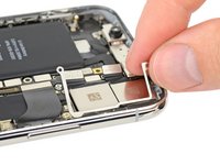
There's a mysterious chip between the Taptic Engine and lower speaker—we're curious to see what's down there!
-
-
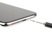
Ferramenta utilizada neste passo:iOpener$17.99
-
This pentalobe looks weirdly unfinished. The bottom screws are more like pins if we're honest.
-
This screw moves the threaded section from the display to the steel frame, and extends the unthreaded section into a freakishly long pin.
-
Our best guess is that this allows the display a bit of flexibility, while also allowing it to move its mounting bracket toward the interior of the phone, incidentally making room for a beefed-up Lightning connector.
-
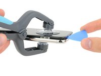
Luckily, it looks like they haven't rearranged too much else, as our typical trifecta of iOpener, iSclack, and iFixit Opening Picks works as in the past.
-
That means no significant change in resistance, and the OLED is well supported by a frame, unlike some displays we know.
-
-
Ferramenta utilizada neste passo:Mako Driver Kit - 64 Precision Bits$39.95
-
Looks like sideways-opening iPhones are here to stay. Apple surprised us with this little trick on the 7 Plus, but by now it's standard.
-
This single bracket covers every logic board connector—we've never seen this kind of connector density.
-
And once again, we're faced with tri-point screws standing sentry over any repairs once you get past the pentalobe screws guarding the door.
-
-
-
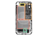
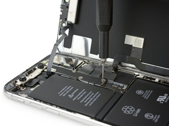
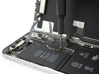
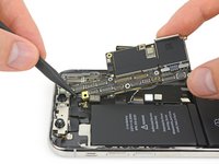
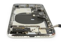
After freeing the massive unibracket from the logic board, we can finally steal a peek at the hardware powering Cupertino's latest flagship.
-
We'll get a better look at the hardware on the display later, for now we satisfy ourselves with an X-ray—turns out that mystery chip is mounted to the display!
-
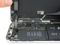
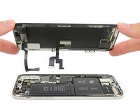
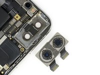
For a change of pace, the display lifts off and leaves the front-facing camera behind.
-
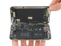
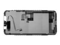
This body shot confirms the layout we observed in our X-Ray recon: most real estate is occupied by the new dual-cell battery, and the logic board has shrunk significantly.
-
-
-
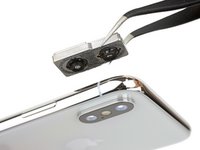
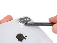
The dual rear camera has a beefy bracket that looks like it might offer some bendgate-proofing support for the delicate components.
-
The cameras are additionally secured to the rear case with some foam adhesive to keep things from jostling out of place. These cameras really need to stay put for Portrait Mode and similar features to work their magic.
-
Surrounding the camera housing cover glass, you can see tiny spot welds likely holding the walls of the camera bump to the case.
-
-
-
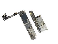
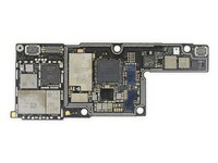
We finally free this most-dense of logic boards to get a closer look.
-
This miniaturized logic board is incredibly space efficient. The density of connectors and components is unprecedented. Ounce for ounce, even an Apple Watch has more bare board.
-
The compact iPhone X board manages to pack more tech and still make the iPhone 8 Plus board to its left look gangly and expansive.
-
Comparing the footprint of the two boards, the iPhone X motherboard is about 70% of the size of the iPhone 8 Plus board—that's a lot more floor space for battery.
-
-
-
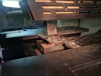
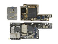
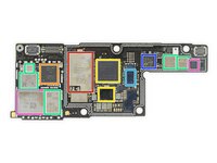
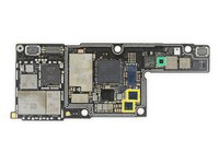
How did Apple put even more tech in 70% of the footprint? By folding the board in half, of course.
-
The two halves are soldered together, so we got some help from our hosts Circuitwise and their BGA hot air rework station to separate the layers.
-
With the pieces separated, we tallied the area of all of the separate layers, and added it up to 135% of the iPhone 8 Plus logic board's area. Way to go putting more into less, Apple.
-
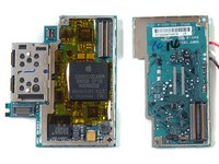
The iPhone X logic board is the first double-stacked board we've seen in an iPhone since the very first iPhone (third photo).
-
-
-
-
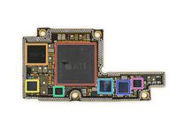
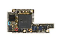
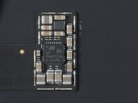
On the first half:
-
Apple APL1W72 A11 Bionic SoC layered over SK hynix H9HKNNNDBMAUUR 3 GB LPDDR4X RAM
-
Apple 338S00341-B1 power management IC
-
Texas Instruments SN2501 battery charger
-
NXP Semiconductor CBTL1612A1—Likely an iteration of the 1610 tristar IC
-
Apple 338S00248 audio codec
-
STMicroelectronics STB600B0 power management
-
Apple 338S00306 power management IC
-
-
-
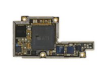
Apple/Murata USI 170821 339S00397 WiFi/Bluetooth module
-
Qualcomm WTR5975 gigabit LTE transceiver.
-
Qualcomm MDM9655 Snapdragon X16 LTE modem and PMD9655 PMIC. But Apple is dual-sourcing the modem, and TechInsights found an Intel XMM7480 (PMB9948) in their A1901 model. Even though the modem is capable of it, Apple isn’t supporting Gigabit speeds with the Qualcomm part.
-
Skyworks SKY78140-22 power amplifier, SKY77366-17 power amplifier, S770 6662, 3760 5418 1736
-
Broadcom BCM59355 wireless charging controller
-
NXP 80V18 PN80V NFC controller module
-
Broadcom AFEM-8072, MMMB power amplifier module
-
-
-
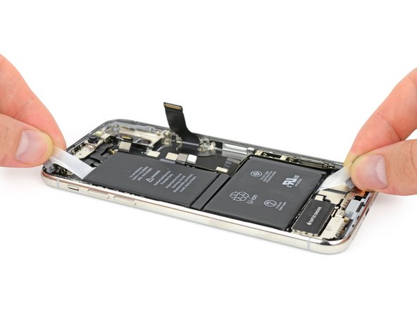
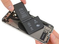
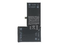
The new dual-celled battery has four pull-tabs, similar to the shorter ones we found in the 8 series, albeit in an entirely new orientation.
-
This phone is packing a 10.35 Wh (2716 mAh at 3.81 V) battery, just beating out the 10.28 Wh 8 Plus battery—but still trailing the Galaxy Note8 with its 12.71 Wh behemoth.
-
The dual-cell design is more of a space-utilization measure than a capacity-changing one. Two cells allows for more creative shapes and placement, to best take advantage of the space left over by shrinking the logic board.
-
-
-
Hey remember that Face ID feature? In an unusual turn of events, we actually tested it before we tore the phone down. Turns out our IR-enabled video camera isn't fast enough to snag the dot pattern, but we can see the illumination alright!
-
History time: way back in the day, Microsoft made a nifty spatial sensor called the Kinect. The infrared dot matrix tech powering it was created by Israeli tech company PrimeSense.
-
Apple bought PrimeSense for a cool $360 million way back in 2013, and has surely invested hundreds of millions more since then bringing this to market.
-
Meanwhile, Microsoft was left in the lurch and had to scramble to develop a new sensing system for the Kinect 2. Perhaps now that the iPhone has a depth sensor, people will attach it to drones, too!
-
-
-
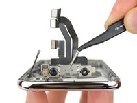
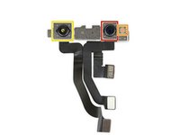
We turn our attention to the top of the phone to find the much anticipated
mini KinectTrueDepth camera system! This system rallies a team of sensors to bring facial recognition to the X. -
Step one in this system: the flood illuminator embedded in the display blasts your face with infrared (IR) light.
-
Next, the front-facing camera, marked in red, confirms the presence of a face.
-
Then the IR dot projector, far right, projects a grid of dots over your face to create a three-dimensional map.
-
Finally, the IR camera on the left reads this map, and sends the data to the phone.
-
Under the hood, the X works some seriously fast software magic to bring all these pieces together and figure out if you're you, or your evil twin.
-
-
-
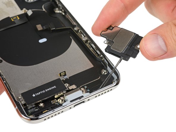
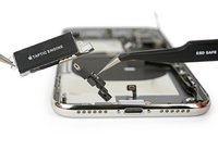
The end is in sight, and we're powering through the remaining components in the rear case.
-
This first little bracket is covered in spring connectors and EMI grounding fingers, and has a ribbon cable stuck to the back.
-
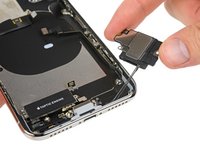
Next out is the lower speaker enclosure, replete with ooey gooey waterproofing adhesive around the port.
-
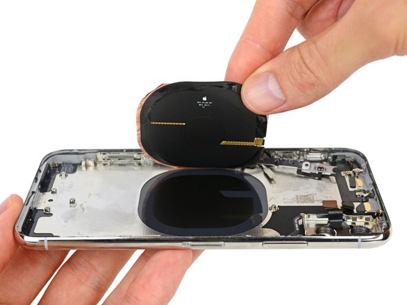
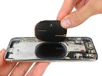
And lastly, the Taptic Engine and famed barometric vent are freed. Apple's Taptic Engine continues to be a linear oscillator vibration motor.
-
-
-
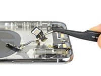
In fine form as always, our teardown engineer demonstrates dual tweezer technique to remove the Lightning connector.
-
Good news for anyone with the wiggly charging cable blues: the Lightning connector is looking extra-reinforced, with a wider bracket that screws into the sidewall of the frame.
-
It also features through holes for the exterior pentalobe screws to pass through and key into the display, as we saw earlier.
-
-
-
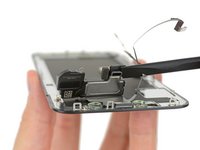
With the main assembly picked to bits, we turn our attention back to the display. The first thing to pop out at us is the earpiece speaker, newly redesigned with a cool duct to channel sound out of the display.
-
Carefully extricating the upper display components yields the most complex upper display component collection we've seen yet. It's home to a loudspeaker, microphone, ambient light sensor, flood illuminator, and proximity sensor.
-
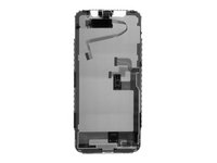
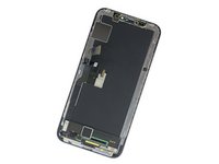
After picking off all the modular bits, we're left with a bare display.
-
-
-
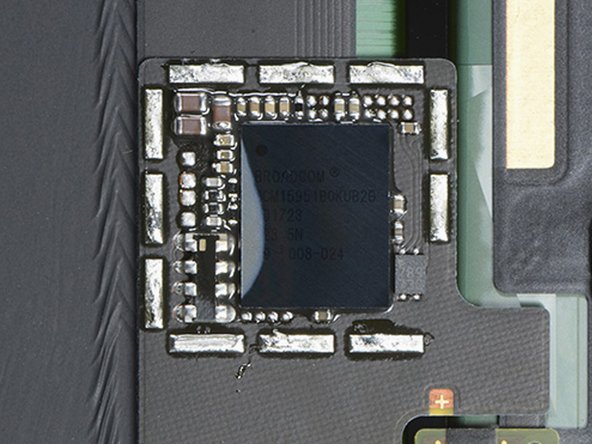
Time to get a look at that mystery chip! With a little help from our friends at TechInsights, we get a peek under the shields on the back of the display and find:
-
A Broadcom touch screen controller, labeled BCM15951B0KUB2G.
-
Also along for the ride: a new STMicro device we have not seen before, an OLED PMIC labeled 10 THADT733 X-139U.
-
-
-
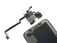
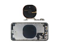
Getting down to the X's bare metal, we run into another familiar piece to this densely-packed puzzle: the wireless charging coil.
-
Oh, and everything attached to it, including the volume buttons, ring/silent switch, and an unidentified sensor bracket.
-
We also peel out the other crazy multi-function cable from the top of the phone. This assembly's home to the quad-LED True Tone flash and the power button, much like iPhones of yore.
-
-
Ferramenta utilizada neste passo:Jimmy$7.95
-
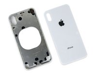
Bonus round: What happens when you break the rear glass on your brand new iPhone X?
-
After lots and lots of heat, we sheathed the spudger and drew our Jimmy. Like the iPhone 8 and 8 Plus, The X features a seriously glued rear panel.
-
After all of our careful Jimmying, we're still stuck: Unlike the iPhone 8's single piece rear panel, the camera bump overlaps the rear glass, and is meticulously welded to the metal frame beneath.
-
In this classic hand-stuck-in-cookie-jar situation, we can either cut off our hand (the camera bump) or shatter the cookie jar (the rear glass). Great.
-
-
-
We hope you enjoyed your 22-course teardown meal. We found it very nutritious.
-
In case you missed the iPhone 8 or iPhone 8 Plus teardowns, you can check those out for some comparisons. And feel free to check out our Smartphone Repairability list for past device scores as well.
-
Thanks once again to our handy helpers, Circuitwise, Creative Electron, and TechInsights!
-
- Display and battery repairs remain a priority in the iPhone's design.
- A cracked display can be replaced without removing the biometric Face ID hardware.
- Liberal use of screws is preferable to glue—but you'll have to bring your Apple-specific drivers (Pentalobe and tri-point) in addition to a standard Phillips.
- Waterproofing measures complicate some repairs, but make difficult water damage repairs less likely.
- Fussy cables tie unrelated components together into complex assemblies—expensive and troublesome to replace.
- Glass on front and back doubles the likelihood of drop damage—and if the back glass breaks, you'll be removing every component and replacing the entire chassis.


Considerações finais
Índice de reparabilidade


(10 é o mais fácil de reparar)
146 comentários
Incredible and dense tech inside this iPhone - thanks ifixit!
Wow! So exciting!
Hello,
Could you give us more info about NFC antenna localization? I suppose it’s on top of the back panel (to avoid conflict with Qi )
Thanks
It’s the top bezel itself, as always.
Tom Chai -
From Iphone 6 to XS Max, its always been on top?