-
-
Start with the back side and use a TR6 bit to remove the four screws (circled in red).
-
-
-
Remove first cover by carefully prying (e.g. with an old (credit) card)
-
It should not take much force
-
In the created opening, roughly where the red square marking is, there is a small plastic latch/hook.
-
Lightly press it down and pry on the back cover with the bluetooth logo.
-
This is the hardest step. Be patient and careful.
-
There is two more latches/hooks, these should not pose a big problem once the first one came lose.
-
-
-
-
Carefully slide out the electronics.
-
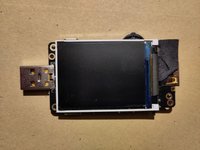
You can see a screen on a PCB in a black plastic frame.
-
Remove the PCB from the frame
-
Remove the black foam tape
-
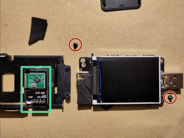
Remove the two screws (redcircles) next to the USB-A connectors.
-
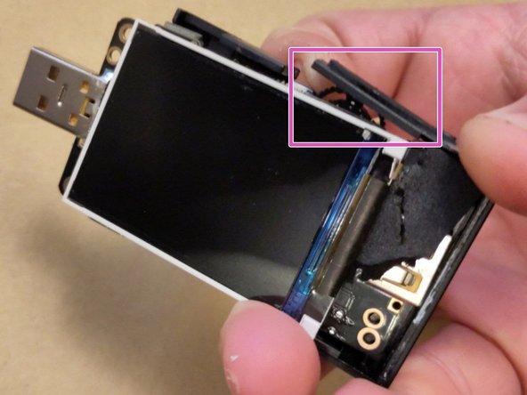
Carefully bend the plastic (pink rectangle) on the menu select button to remove the PCB.
-
If you have the FNB58B variant you should see the bluetooth module remain in the frame (green square).
-
-
-
Screen labelled "NFP200H-20A", could not identify further. Probably some standard TFT display with SPI/I2C.
-
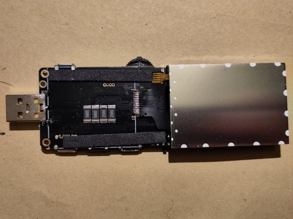
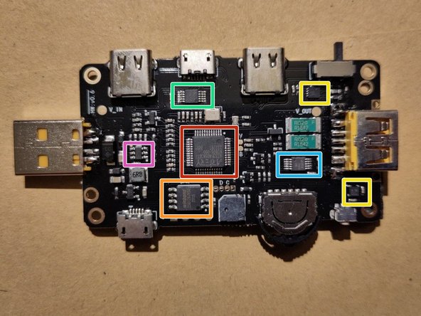
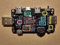
Backside main PCB:
-
Red square: Artery AT32F403A CGT7 (Main microcontroller) with orange square: W25Q128JV (128M-bit Serial Flash Memory with uniform 4KB sectors and Dual/Quad SPI)
-
Blue square: 3PEAK TPA626 TPA626 (Bi-Directional Current and Power Monitor)
-
Green square: RS2228 MCO7117 (High-Speed USB 2.0 (480-Mbps) 1:2 Multiplexer/Demultiplexer Switch). Probably to switch between the USB micro and -C inputs.
-
Pink square: IC labelled IV7NS. I think it might be a MPS MP2451DT step-down converter. Probably to always provide the 3.3V logic-level voltage for the ICs.
-
Yellow squares: could not identify. One (presumably) QFN14 labelled "UAAC CEH" and one with unknown form factor "WL5 J3".
-
Bluetooth board: pogo-pins to make contact to main board and Tuya BEKEN BK3432
-


5Comentários do guia
What is the marking on the resistor? to the middle right of the yellow square connected to pin 7, mine shorted out and is illegible.
I figured out the Bluetooth protocol for this if anyone wants a good way to log this without their crappy software. https://gist.github.com/parkerlreed/0ce4...
Thank you for your work :D
Pota-to -
UAAC CEH скорее всего FUSB302BMPX. wl5 j3 это точно kxtj-1057 акселерометр, проверено заменой.
Had the four 20R0 chips behind the screen let magic smoke out, thought I was finished but opened it up cleaned up some crispy bits (ok a lot of bits) slapped some thermal paste all over it and put it together and wtf it works fine still? Smells like electronic doodoo, just very surprised behind my screen so much crispy FNB58 and still accurate and working. Eh happy testing. :)